Home What Is a Neurosynaptic Chip? Definition, Architecture, and Applications
What Is a Neurosynaptic Chip? Definition, Architecture, and Applications
Learn what a neurosynaptic chip is, how it mimics biological neural networks in silicon, why it matters for AI efficiency, and where it is used across industries.
What Is a Neurosynaptic Chip?
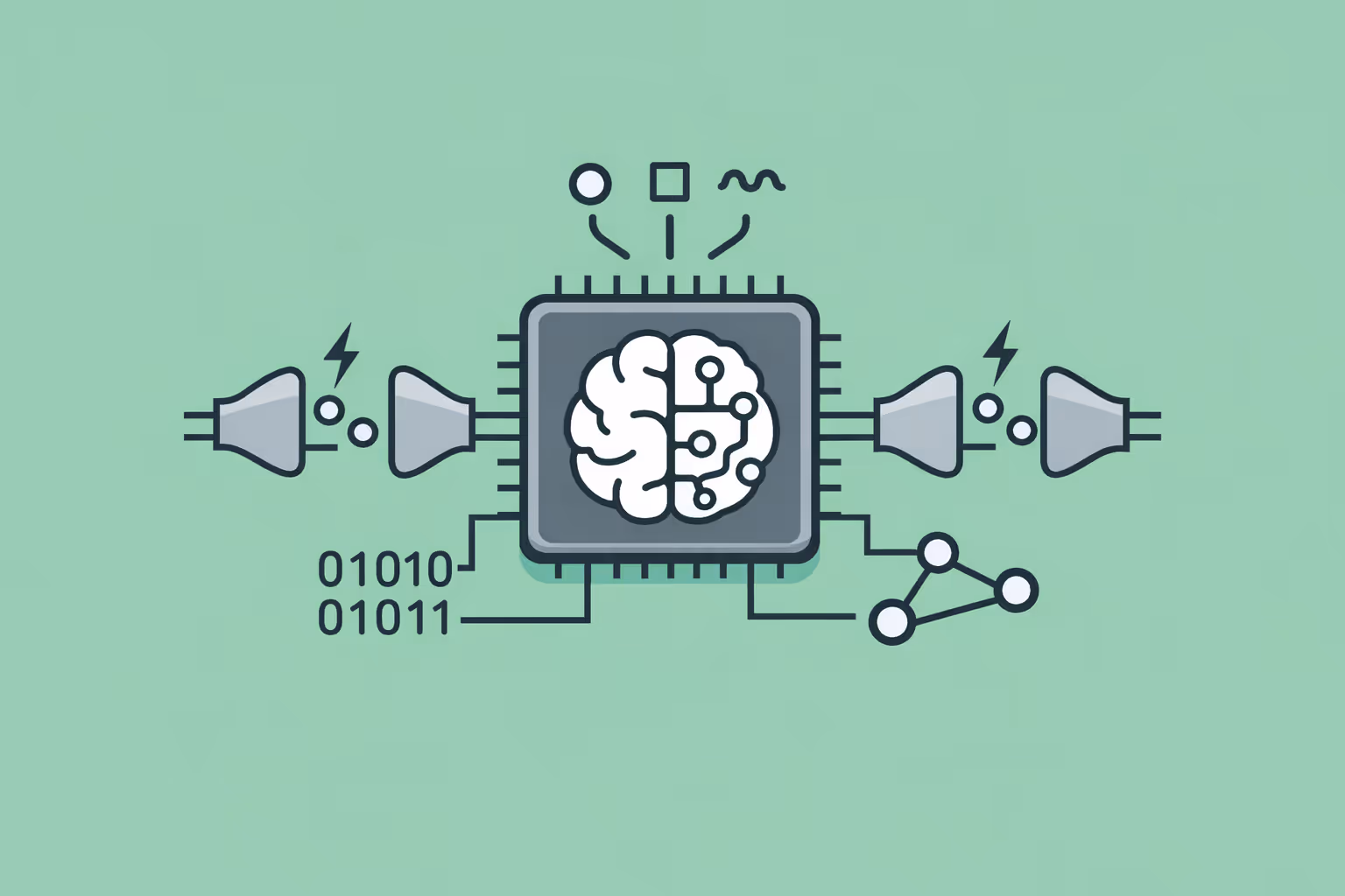
A neurosynaptic chip is a type of processor designed to mimic the structure and signaling behavior of biological neurons and synapses. Unlike conventional processors that execute sequential instructions through a central clock cycle, a neurosynaptic chip organizes its transistors into networks of artificial neurons connected by programmable synapses.
Each neuron on the chip can receive inputs, accumulate signals, and fire outputs to neighboring neurons, replicating the parallel, event-driven processing that occurs in the human brain.
The term "neurosynaptic" combines two foundational elements of biological computation. Neurons are the cells that process and transmit information through electrical impulses. Synapses are the junctions between neurons where signals pass from one cell to another, strengthening or weakening over time based on activity.
A neurosynaptic chip encodes both of these elements directly in hardware, creating a physical substrate that processes information through spiking patterns rather than binary arithmetic.
This approach falls under the broader discipline of neuromorphic computing, which encompasses all hardware and software architectures inspired by the nervous system. The neurosynaptic chip is one of the most concrete implementations of that vision.
IBM's TrueNorth processor, introduced as a research milestone, demonstrated that a single chip could integrate over one million programmable neurons and 256 million configurable synapses while consuming only 70 milliwatts of power. That power figure is orders of magnitude lower than what a traditional GPU or CPU would require for comparable pattern recognition tasks.
The significance of neurosynaptic chips extends beyond raw performance. They represent a fundamentally different model of computation, one that prioritizes energy efficiency, real-time sensory processing, and adaptive learning over brute-force arithmetic throughput.
For workloads involving artificial intelligence, particularly perception, classification, and temporal pattern detection, this architecture offers advantages that conventional chip designs struggle to match.
How Neurosynaptic Chips Work
Understanding neurosynaptic chips requires examining three layers: the neuron model, the synaptic interconnection fabric, and the event-driven communication protocol that ties everything together.
The Neuron Model
Each artificial neuron on a neurosynaptic chip is a small computational unit that accumulates incoming signals over time. When the accumulated charge crosses a defined threshold, the neuron "fires," producing a spike that propagates to connected neurons. After firing, the neuron resets its internal state and enters a brief refractory period before it can fire again.
This integrate-and-fire behavior mirrors how biological neurons operate, where the timing and frequency of spikes carry information rather than static voltage levels.
The key difference from traditional logic gates is that neurosynaptic neurons are stateful. They maintain an internal membrane potential that changes with every incoming spike. This statefulness allows the chip to process temporal patterns, sequences of events unfolding over time, without requiring an external memory hierarchy or clock-driven scheduling.
Synaptic Connections
Synapses on a neurosynaptic chip are programmable connections between neurons. Each synapse has a weight, a numerical value that determines how strongly one neuron's output influences another neuron's input. Positive weights cause excitatory effects, pushing the receiving neuron closer to its firing threshold. Negative weights cause inhibitory effects, suppressing activity.
The synapse weights are typically stored in local memory arrays embedded alongside the neuron circuits. This colocation of memory and processing is a defining characteristic of neurosynaptic architecture. In conventional computers, data must travel between a separate memory unit and the processor, creating the von Neumann bottleneck that limits throughput and wastes energy.
Neurosynaptic chips avoid this bottleneck by keeping data and computation physically adjacent, a principle shared with other forms of neural net processors.
Event-Driven Processing
Conventional processors operate on a global clock. Every cycle, every transistor switches state regardless of whether useful work is being performed. Neurosynaptic chips operate asynchronously. A neuron consumes energy only when it receives a spike or fires one. If a region of the chip has no active inputs, it sits idle at near-zero power consumption.
This event-driven model is what enables the dramatic energy efficiency of neurosynaptic architectures. In sensory processing tasks, such as monitoring a video feed for unusual motion, most of the input is static background. A conventional processor analyzes every frame in full. A neurosynaptic chip responds only to changes, activating neurons in proportion to the amount of new information arriving at the sensors.
The result is a system that scales its energy use with the complexity of the input rather than the resolution of the sensor.
The spikes themselves carry information through their timing relative to other spikes. This temporal coding scheme enables the chip to represent and process continuous, real-world signals with high fidelity. It is particularly well suited for tasks like audio recognition, motion detection, and sensor fusion, all of which involve interpreting patterns that evolve over time.
| Component | Function | Key Detail |
|---|---|---|
| The Neuron Model | Each artificial neuron on a neurosynaptic chip is a small computational unit that. | When the accumulated charge crosses a defined threshold |
| Synaptic Connections | Synapses on a neurosynaptic chip are programmable connections between neurons. | — |
| Event-Driven Processing | Conventional processors operate on a global clock. | Monitoring a video feed for unusual motion |
Why Neurosynaptic Chips Matter
Neurosynaptic chips address several limitations of conventional hardware that become increasingly apparent as artificial intelligence scales into power-constrained and latency-sensitive environments.
Energy Efficiency
The power consumption gap between neurosynaptic chips and traditional processors is substantial. Training and running deep learning models on GPUs requires hundreds of watts per chip. Data centers housing thousands of these chips consume megawatts of electricity and require extensive cooling infrastructure.
Neurosynaptic chips performing inference on sensory data can operate in the milliwatt range, making them viable for battery-powered devices, remote sensors, and wearable technology.
This efficiency is central to the vision of sustainable AI. As AI deployment expands across billions of devices, the aggregate energy demand becomes a material concern. Hardware that can deliver intelligent behavior at a fraction of the energy cost fundamentally changes the economic and environmental calculus of deploying AI at scale.
Real-Time Responsiveness
Because neurosynaptic chips process spikes as they arrive rather than waiting for batch computations to complete, they achieve extremely low inference latency. For applications in edge AI, where decisions must happen at the point of data generation without round-trip communication to a cloud server, this responsiveness is critical.
Autonomous drones, industrial safety systems, and prosthetic devices all require sub-millisecond reaction times that align naturally with the event-driven processing model.
Scalability Through Modularity
Neurosynaptic chips are typically designed as arrays of identical neurosynaptic cores, each containing a fixed number of neurons and synapses. These cores communicate through a network-on-chip routing fabric. To build larger systems, engineers tile multiple chips together, extending the neural network across chip boundaries. This modular approach mirrors how biological brains scale, by adding more cortical columns rather than making a single column larger.
The modularity also simplifies manufacturing and system design. Each core is self-contained, reducing the complexity of global wiring and enabling fault tolerance. If one core fails, the network can route around it, a resilience property that conventional processor designs do not inherently provide.
Bridging Hardware and Biology
Neurosynaptic chips serve as a research platform for computational neuroscience. By implementing biologically plausible neuron and synapse models in silicon, researchers can test hypotheses about how neural networks in the brain encode, store, and retrieve information.
The hardware provides a testbed that operates at speeds far exceeding biological real time, accelerating experiments that would take prohibitively long in software simulation.
This bidirectional relationship between neuroscience and chip design means that advances in understanding the brain can feed directly into improved chip architectures, and observations from chip behavior can generate new neuroscience hypotheses.
Neurosynaptic Chip Use Cases
Neurosynaptic chips are not general-purpose replacements for CPUs or GPUs. They excel in specific application domains where their architectural strengths, energy efficiency, temporal processing, and event-driven operation, provide a decisive advantage.
Sensory Processing and Pattern Recognition
The most natural application for neurosynaptic chips is processing data from sensors: cameras, microphones, accelerometers, chemical detectors, and similar inputs. Tasks like image classification, voice activity detection, gesture recognition, and environmental monitoring map directly onto spiking neural network architectures.
The chip processes sensory streams continuously, detecting patterns and anomalies in real time with minimal power draw.
Autonomous Robotics
Robots operating in unstructured environments need to perceive their surroundings, plan movements, and react to unexpected obstacles with low latency and limited energy budgets. Neurosynaptic chips enable onboard perception systems that process visual and tactile input without relying on cloud connectivity.
Small mobile robots, drones, and underwater vehicles benefit from the combination of low power consumption and real-time sensory processing that these chips provide.
Internet of Things and Smart Infrastructure
IoT deployments often involve thousands of distributed sensors operating on battery power or energy harvesting. Neurosynaptic chips enable intelligent sensing at each node, allowing devices to filter, classify, and respond to environmental data locally. This reduces the need to transmit raw data to a central server, cutting bandwidth costs and improving response times. Smart buildings, precision agriculture systems, and environmental monitoring networks are practical deployment contexts.
Medical Devices and Neural Interfaces
Neurosynaptic chips are uniquely suited for brain-computer interfaces and implantable medical devices. Their spiking architecture is natively compatible with the electrical signals produced by biological neurons, simplifying the translation between neural recordings and digital processing. Low power consumption is essential for implanted devices where battery replacement requires surgery.
Applications include neural prosthetics, seizure prediction systems, and adaptive deep brain stimulation controllers.
Defense and Surveillance
Military and security applications require AI systems that operate in size-constrained, power-limited, and communication-denied environments. Neurosynaptic chips enable onboard intelligence for unmanned aerial vehicles, portable threat detection systems, and autonomous sensor networks deployed in remote locations. The ability to process sensor data without transmitting it also provides operational security by minimizing the electronic footprint of the system.
Cognitive Computing Systems
Neurosynaptic chips contribute to the broader field of cognitive computing, where systems are designed to simulate human thought processes in decision-making. Platforms like IBM Watson have explored integrating neuromorphic principles to handle ambiguous, context-dependent reasoning tasks that traditional architectures find computationally expensive.
Challenges and Limitations
Neurosynaptic chips are a maturing technology. Several obstacles stand between current capabilities and widespread commercial adoption.
Programming Model Complexity
Conventional processors benefit from decades of software toolchains, programming languages, compilers, and developer training. Neurosynaptic chips require fundamentally different programming paradigms. Developers must think in terms of spiking neural network topologies, spike timing, and synaptic learning rules rather than loops, conditionals, and memory addresses.
The ecosystem of development tools, debuggers, and libraries for neurosynaptic hardware is still nascent compared to what exists for CPUs and GPUs.
This programming gap limits adoption. Engineers trained in conventional machine learning frameworks cannot transfer their skills to neurosynaptic platforms without significant retraining. Until high-level abstractions and automated mapping tools mature, development costs will remain higher than for conventional AI accelerator hardware.
Limited Precision for Some Workloads
Neurosynaptic chips encode information in spike timing and frequency rather than in high-precision floating-point numbers. For tasks that require exact numerical computation, such as financial modeling, scientific simulation, or large-scale matrix algebra, this encoding scheme introduces accuracy limitations. The chips are optimized for perception and classification tasks where approximate, probabilistic outputs are acceptable, not for workloads that demand deterministic arithmetic precision.
Integration with Existing Systems
Most AI infrastructure today is built around conventional processor architectures. Integrating a neurosynaptic chip into an existing data pipeline requires bridging two different computational paradigms. Data must be converted from standard digital formats into spike-encoded representations for the neurosynaptic chip and then converted back for downstream processing. This encoding and decoding overhead can reduce or eliminate the efficiency gains if the system is not designed holistically.
Manufacturing Scale and Cost
Neurosynaptic chips are produced in far smaller volumes than commodity CPUs and GPUs. Limited manufacturing scale translates to higher per-unit costs, which constrains adoption to research institutions, government agencies, and well-funded industrial projects. As demand grows and fabrication processes mature, costs are expected to decrease, but the timeline for cost parity with conventional chips remains uncertain.
Training Spiking Neural Networks
Training algorithms for spiking neural networks are less mature than the backpropagation methods used in conventional deep learning. Spike-timing-dependent plasticity (STDP) and other biologically inspired learning rules show promise but do not yet achieve the same accuracy as gradient-based optimization on standard benchmarks.
Researchers are actively developing hybrid approaches that train models using conventional methods and then convert them to spiking formats for deployment on neurosynaptic hardware, but this conversion process can introduce performance degradation.
The Future of Neurosynaptic Computing
Neurosynaptic computing sits at the intersection of semiconductor engineering, neuroscience, and artificial intelligence. Several trajectories will shape its evolution over the coming decade.
Material and Device Innovation
Current neurosynaptic chips use conventional CMOS transistors to emulate neurons and synapses. Emerging technologies, including memristors, phase-change memory, and spintronic devices, offer the possibility of building artificial synapses from materials that natively exhibit analog, tunable resistance.
These devices could store synaptic weights directly in their physical state rather than in digital memory, further reducing energy consumption and chip area while increasing synapse density by orders of magnitude.
Convergence with Mainstream AI
The boundary between neuromorphic and conventional AI hardware is blurring. Major chip companies are incorporating neural processing units into mainstream processors, and reinforcement learning algorithms that rely on temporal reward signals map naturally onto spiking architectures.
As software tools improve and interoperability standards emerge, neurosynaptic chips are likely to become specialized coprocessors within heterogeneous computing systems rather than standalone platforms.
Expanding Application Domains
As power budgets tighten and AI moves further toward the edge, the demand for ultra-low-power inference hardware will grow. Neurosynaptic chips are positioned to serve emerging applications in always-on wearable health monitors, distributed environmental sensing, space exploration, and next-generation human-computer interfaces. Each of these domains values energy efficiency and real-time responsiveness above raw computational throughput.
Open Research Platforms
The availability of open-source neuromorphic simulators, standardized spiking neural network formats, and accessible research chips from academic consortia is lowering the barrier to entry. More researchers and engineers will gain exposure to neurosynaptic concepts, accelerating the development of practical applications and training a workforce that can bridge the gap between conventional AI and neuromorphic engineering.
Toward Brain-Scale Systems
Long-term roadmaps for neurosynaptic computing envision systems with billions of neurons and trillions of synapses, approaching the scale of the human cortex. Achieving this scale will require breakthroughs in chip interconnect technology, 3D chip stacking, and energy-efficient communication protocols.
While brain-scale neuromorphic systems remain a research aspiration, each generation of neurosynaptic chips moves closer to that threshold, expanding the complexity of problems these systems can address.
The trajectory of neurosynaptic computing is not about replacing existing hardware. It is about expanding the range of environments and workloads where intelligent computation is feasible. For tasks that demand continuous, low-power, real-time processing of sensory data, neurosynaptic chips offer an architectural foundation that conventional processors were never designed to provide.
FAQ
How is a neurosynaptic chip different from a GPU?
A GPU is a massively parallel processor designed for high-throughput arithmetic, particularly matrix multiplications used in deep learning training and inference. It operates on a global clock and processes data in large batches. A neurosynaptic chip uses event-driven spiking neurons that activate only when they receive input, consuming energy in proportion to the information being processed rather than the clock speed.
GPUs excel at training large models with high numerical precision. Neurosynaptic chips excel at real-time, low-power inference for sensory and temporal pattern recognition tasks.
Can neurosynaptic chips run standard deep learning models?
Not directly. Standard deep learning models are designed for synchronous, floating-point computation. Running them on a neurosynaptic chip requires converting the model into a spiking neural network representation. Conversion tools exist, but the process can reduce model accuracy, and not all model architectures convert efficiently.
Research into native spiking network training methods is closing this gap, but for now, neurosynaptic chips are best suited for models designed or adapted specifically for spiking hardware.
What is the relationship between neurosynaptic chips and neuromorphic computing?
Neuromorphic computing is the broad field of building computing systems inspired by the structure and function of biological nervous systems. A neurosynaptic chip is a specific hardware implementation within that field. Other neuromorphic approaches include analog circuit designs, photonic neural networks, and software-based spiking simulators.
The neurosynaptic chip represents one of the most developed and well-known digital implementations of neuromorphic principles.
Who manufactures neurosynaptic chips?
IBM pioneered the category with its TrueNorth chip. Intel developed Loihi and Loihi 2 as neuromorphic research processors. Academic institutions and startups, including BrainChip (with its Akida processor), SynSense, and GrAI Matter Labs, also produce commercial or research-grade neurosynaptic and neuromorphic hardware.
The field remains smaller than the conventional AI accelerator market, but the number of active manufacturers is growing as demand for ultra-low-power AI increases.
Are neurosynaptic chips available for commercial use?
Some neurosynaptic and neuromorphic chips are commercially available. BrainChip's Akida processor can be purchased as a development kit and integrated into production systems. Intel's Loihi 2 is available through research partnerships.
The market is transitioning from research-only availability to broader commercial access, though the ecosystem of tools, integrations, and developer support is still less mature than what exists for GPUs and conventional machine learning hardware.
Further reading

Data Scientist: What They Do, Key Skills, and How to Become One
Learn what a data scientist does, the key skills required, common tools they use, and how to build a career in data science.

Backpropagation Algorithm: How It Works, Why It Matters, and Practical Applications
Learn how the backpropagation algorithm trains neural networks, why it remains essential for deep learning, and where it applies in practice.

Knowledge Graph: Definition, How It Works, and Use Cases
Learn what a knowledge graph is, how it structures relationships between entities, why it matters for AI and machine learning, and how organizations build and use knowledge graphs.
Vision Language Models (VLMs): How They Work, Architectures, and Practical Applications
Learn what vision language models are, how VLMs combine visual and textual understanding, key architectures like CLIP and LLaVA, real-world use cases, and how to get started.
Convolutional Neural Network (CNN): How It Works, Use Cases, and Practical Guide
Learn what a convolutional neural network is, how CNNs process visual data, their real-world applications, and the key limitations practitioners should know.

REALM (Retrieval-Augmented Language Model): What It Is, How It Works, and Use Cases
Learn what REALM is, how it combines retrieval and language modeling for knowledge-intensive NLP, and explore practical use cases, limitations, and how it compares to RAG.